Abstract
- Porting designs to new technology is common and involves schematic porting, sizing, and layout.
- Full custom design’s porting process consumes time, effort, and budget, with risks and uncertainties.
- Sizing and verification, including various factors, are often underestimated in design.
- MunEDA’s WiCkeD tool suite reduced project schedule, improved quality, and enhanced predictability.
- Reference case demonstrates successful application of WiCkeD in design porting.
IP Porting
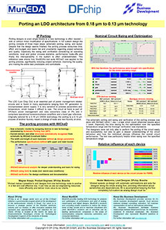
The LDO (Low Drop Out) is an essential part of power management related circuits and is found in many applications ranging from RF generation to microprocessor power supply. It is very sensitive to process parameters and
temperature, which makes it difficult to size.
The circuit at hand is part of DFchip’s power management and data converters class of IPs and it comprises operational transconductance amplifiers and a band gap reference. Originally tailored for a 0.18 μm CMOS technology, the porting to a 0.13 μm process of another foundry meant a change of node and new foundry at once.
For more information on this topic, send us a request
To get the selected information or request for a solutions demo please enter your data with the following form.