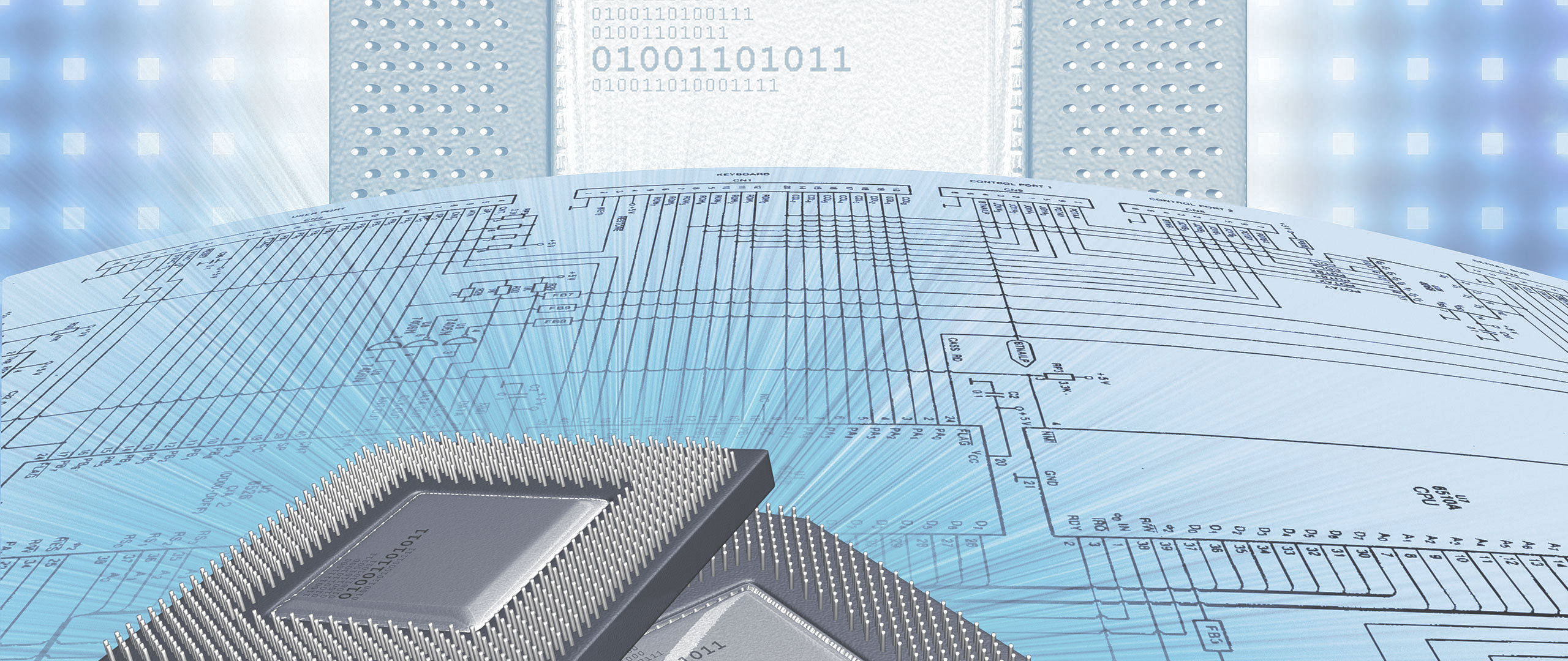
MunEDA Solutions & Applications
Low Power Tuning & Sizing for Custom Circuits (Analog, RF)
Optimize low power custom IC design effortlessly with MunEDA WiCkeD-automated tuning, yield-focused design, and robustness verification for diverse applications.
Memory Design (SRAM, DRAM, Flash, FPGA)
WiCkeD: Optimize memory cell design with high-sigma verification, automated optimization, and 10-100x faster efficiency.
Dependent Simulations & Circuit Trimming
WiCkeD combines results from diverse simulations for accurate analysis and optimization, ensuring consistency in statistical analysis and trimming scenarios.
Standard Cell & I/O Cell Design Optimization
WiCkeD for Standard & I/O Cell Design: Smart, fast, and reliable solutions for optimizing performance under diverse operating conditions, tackling the complexities of standard cell design efficiently.
High-Sigma Verification for SRAM Designs
WiCkeD provides robust yield estimation and high-sigma analysis for critical circuits like SRAM and CRAM, ensuring extremely low failure probabilities in diverse applications from memory to standard cells, ADCs, and PLLs.
Process Characterization & Backward Process Propagation
WiCkeD streamlines Monte Carlo simulation by correlating corner models, simplifying parameter calculations for design and production engineers.
RSM Circuit Modelling & Model Generation
WiCkeD RSM simplifies circuit design, offering response surface models for efficient simulation, optimization, and increased flexibility in analyzing complex circuits within larger systems.
…and many more
- Custom IC Design Migration, Verification & Optimization
- PCM Statistical Parameter Calculation
- Yield Plotting
- Circuit Sensitivity Analysis in FinFET Technologies
- Fast Hierarchical & High Sigma Monte Carlo
- Verification and Characterization of Analog Circuits
- PVT & Worst Case Corner Run Analysis of Custom IC & IP

CTI Renato Archer at MUGM MunEDA User Group Meeting 2023
“With MunEDA WiCkeD we could reduce design time and effort significantly to optimize our control circuits of an LCL for radiation hardening”
Let’s work together on your
next design project
Use MunEDA tools and support to speed up efficiency,
quality and outcome of your next circuit design project