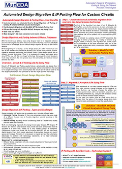
Automated Design Migration & Porting Flow – User Benefits
- Customer proven and automated flow for Design Migration & IP Porting of existing IP between different process technologies
- Fast Schematic Migration with MunEDA SPT Schematic Porting Tool
- Efficient Re-Sizing with MunEDA WiCkeD Analysis and Sizing Tools
- Save Time and Efforts
- Make designer’s life more convenient and results reliable
Design Migration and Porting between Different Processes
With the trend to go fabless, many chip designs have to be migrated between process technologies and within internal and external foundry processes. MunEDA tools solve the challenges of such difficult design migration & sizing for full-custom designs. At the beginning of – or during – a new design project, it is often necessary to use and re-use available IP (intellectual property) and circuits from previous projects, instead of designing everything from scratch. Often a new design uses a new or different process technology. Thus, it is necessary to migrate and apply given circuit IP for use with this new target technology. Consequently, circuit designers must adapt circuits to the new process by a time-consuming and tedious manual process very often.
For more information on this topic, send us a request
To get the selected information or request for a solutions demo please enter your data with the following form.