Memory Design (SRAM, DRAM, Flash, FPGA) using WiCkeDTM
WiCkeD for Memory Cell Design – User Benefits
- Applicable for all kind of memory design (SRAM, DRAM, Flash, FPGA, …)
- Analysis of process variations and high-sigma verification
- Memory cell & interface optimization with automated sizing and yield optimization
- 10-100x faster and more efficient than pure manual design
Challenges in Memory Design
Many building blocks of memory (SRAM, DRAM, Flash, FPGA) are very sensitive to process variation, supply voltage, leakage and mismatch. Top challenge for memory designers are therefore to analyze and optimize the circuit robustness at high levels beyond six sigma, for memory circuits that are sensitive to process variation, supply voltage, leakage and mismatch. Typical Circuits for memory design are therefore memory cells (bit cells), sense amplifiers, charge pumps, oscillators, receiver paths, decoders, timers, bandgap references, multiplexers and other circuits. Typical performance metrics for memory designs are e.g. write time, static noise margin, leakage current, power consumption, glitch, offset, accuracy, delays, pin-to-pin-skew and many more.
SRAM, CRAM
SRAM & CRAM bit cells require high sigma robustness for local variation (OCV) because they are instantiated in large numbers on a chip on the die, the impact of random local variation must be analyzed to a high sigma level. Large SRAM arrays require robustness levels of 6.5 sigma and higher.
Monte Carlo needs a too large sample size for such high sigma levels due to the long tail distributions of key metrics. To determine the failure rate in the order of one part-per-billion (6 sigma) with 10% error, the sample size has to exceed 380 billion runs what is not realistic to achieve with Monte Carlo based methods. MunEDA WiCkeD delivers highly efficient methods for bit cell analysis & optimization.
DRAM
DRAM designs are highly influenced on short time process changes in the fab. Therefore the fast analysis of existing DRAM chips and underlying circuits is key for successful yield enhancement already in design. As mainly influenced by process variation timing and power are key influence factors for DRAM designs and interfaces. For this reason it is important to design the cells and sensing circuits in a way that it is as much insensitive against the process variations as possible. For this reason highly efficient sensitivity & yield analysis and optimization methods are required. MunEDA WiCkeD delivers highly efficient methods for analysis & optimization of memory interfaces and sensing circuits.
Flash
Flash is a non-volatile memory that is widely used in USB, microSD, SSD, mobile memory, navigation, digital devices and many more. Based on technology progress flash memory is underlying a constant cell size reduction based on process and design shrink. The reduced margin between the cell distributions lead often to an increased read error rate. Therefore the analysis and optimization of the variation and sensitivity of the read sense amps is very important for good performing and high-yielding flash memory. MunEDA WiCkeD delivers highly efficient methods for design shrink, analysis & optimization of flash memory.
FPGA
FPGA designs are highly dominated by leading-edge process technology and therfore face an agressive development schedule. FPGAs consist of ultra-high density of meanwhile up to billions of transistors or core cells (e.g. CRAM) within the FPGA core with additional transceivers, PCIe hard IP and general-purpose highspeed IOs. For this reason a very specific sigma-variation-stability is required to avoid both underesign that cost yield loss and also expensive overdesign. For FPGA designs therefore methods like sensitivity analyis and worst case analysis are key for core cell design to detect the influence of static noise or mismatch. The interface designs (transceivers, high-speed IOs) and LUT (look-up tables) require highly efficient performance and yield optimization methods to reduce area and keep the delays under control. Both are included in MunEDA WiCkeD tool suite and proven with FPGA developers worldwide since years.
MunEDA WiCkeD tools for memory cell (bit cell) high-sigma parametric yield verification (SRAM, CRAM)
FPGA designs are highly dominated by leading-edge process technology and therfore face an agressive development schedule. FPGAs consist of ultra-high MunEDA’s advanced worst-case analysis (WCA) methodology is the most efficient way to let the user determine realistic and accurate high sigma worst-case conditions of margins, leakage, write times and other metrics.
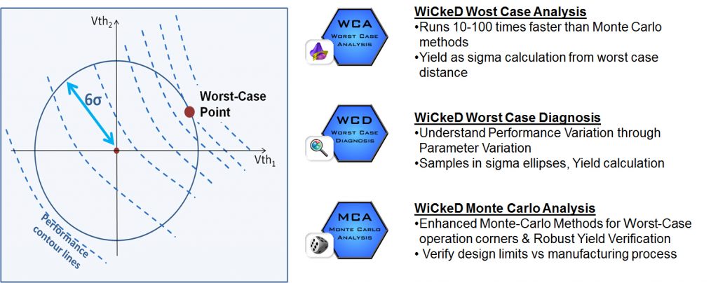
Realistic worst-case bit cell net lists enable failure rate estimation of whole columns and arrays. Particularly for problems with non-linearly bounded failure regions, MOS model discontinuities or multiple failure regions, adaptive WCA tools are more reliable and accurate than choosing sample points by one global response surface model. To compare results, response surface models and importance sampling are available for WiCkeD.
MunEDA WiCkeD Tools for Memory Interface Development
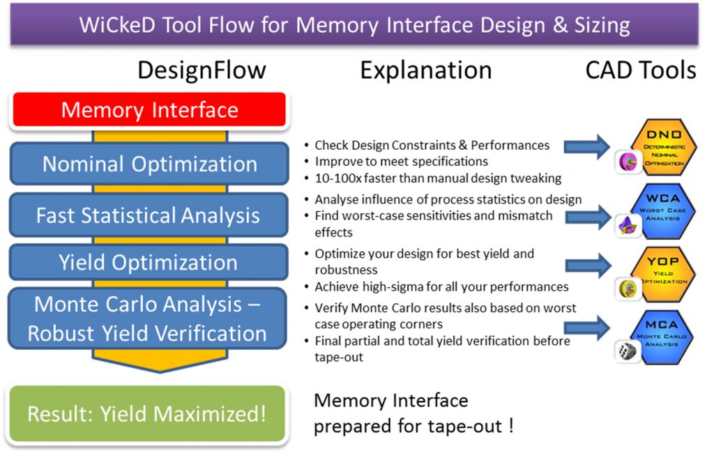
Designing and verifying high-speed low power memory interfaces such as LPDDR is a challenge for full custom designers. MunEDA WiCkeD provides advanced statistical analysis methods and optimization software to tune I/O circuits for low jitter, duty cycle, low power, reliability and parametric robustness.
MunEDA WiCkeD delivers numerous highly efficient tools for design migration, analysis, and sizing of memory cells and memory interfaces. All tools are proven within the last 10+ years in tape-out and silicon by the leading memory making companies worldwide (See also references below). MunEDA WiCkeD fills the functionality gap in existing design frameworks and simulators especially in the memory design area.
MunEDA WiCkeD – Technology Support
- WiCkeDTM & SPT Design Tool Suites
- Integrated into standard design environments
- For more information and support contact www.muneda.com
Infineon at MUGM MunEDA User Group Meeting 2023
“MunEDA WiCkeD supports us to solve the main challenges in SRAM design like shrinking transistor geometries, process variation, power consumption, density, soft errors”
Let’s work together on your
next design project
Use MunEDA tools and support to speed up efficiency,
quality and outcome of your next circuit design project